Showing posts with label AR2. Show all posts

29 September 2023

UPDATE: Life ;^)

Feels odd to realize that it's been 9 months since the last update, and oh boy what an interesting 9 months it's been... But through all this chaos we have managed to make some fun memories with the little one, memories that somehow feel that bit more special then before ðŸ¥²

One thing we quickly realised is that we have way less time on our hands (surprise surprise), as our "free" time is now either catching up on chores/admin or trying to recharge our mental batteries. But as always we have found ways to adapt to the new situation (or so we claim), whether it be by improving project workflow/tracking or outsourcing tasks where/when possible.

So in this update I want to first talk about the former, improving project workflow, specifically how I now plan to use Altium Designer when working on PCBAs. Then to finish things off, I will show some snapshots of projects I have miraculously found the time to work on :O


Altium Designer Workflow & Templates

Looking back, my PCBA design workflow was not that efficient, which I guess was not a huge deal at the time... But now that free time is that bit harder to come by, I have tried to optimize a number of aspects. For example:

Old workflow

Revised workflow

Altium component creation & management

A SCH symbol & PCB footprint would be linked up in a relevant schematic library (SchLib), of which there were 12 (res, cap, IC…).

SCH symbols would typically be reused, but would be copied from one component to another. So updating a SCH symbol used by many components was very tedious as I had to update each one manually.

PCB footprints would always be created from scratch, as I could not easily check if a footprint already existed until I generated it (usually via IPC Compliant Footprint Wizard).

All components are now managed by a single database library (DbLib), which I edit via Microsoft Access. This makes it very easy to link up a single SCH symbol and/or PCB footprint to many components, so creating a new component is now much quicker. 

Since everything is linked up by a database, if I want to update a SCH symbol or a PCB footprint that's used by many parts all I have to do is make a single edit.

Lastly, PCB footprints (and their name) are created based on manufacturers recommendation (vs going direct to IPC Compliant Footprint Wizard). Making it easier to see if an existing footprint is present in the database.

Altium project creation

When creating a new Altium PRJ, I would first try to find a previous project that somewhat resembled what I was hoping to achieve. Then I would manually copy and modify all the project files (SCH, PCB, BOM…) & individual parameters… Inevitably missing something crucial along the way.

I now have an Altium PRJ template which automatically adds all relevant files (SCH, PCB, BOM…) when a project is created. Plus, all linked files now reference the project parameters, making it very easy to update project revisions & release datapacks.

Altium project release (datapack generation)

Once a project was finalised, I would manually go over all line items in the ActiveBOM and allocate a manufacturing part number to those that did not have one (like jelly bean resistors & capacitors that used a generic component).

With the ActiveBOM configured I would then create the project datapack (PCB FAB & ASSY files) by manually generating each output container in the OutJob. With 7 containers this meant 7 individual clicks, not including setting up the container names.

Now that all components are managed by a database library (DbLib), it's much easier to lock in the key details (MPN plus two alternative) during component creation. So, no more fiddling with ActiveBOM where MPN info would be lost between projects.

Lastly, datapack generation is now handled by the Project Releaser, which configures the output containers (PCB FAB, PCB ASSY, PRJ validation & snapshot…) based on project parameters. Letting me generate a datapack with the click of a single button :D

With all that said, the next step is to use the revised workflow & templates for my Prusa XL side filament sensor mod. But since Prusa have not yet shared the design files (like with the MK3S), I will have to get the printer first before I can make any major progress.


Project Snapshots

As promised, here are some snapshots of projects I have found the time to work on:

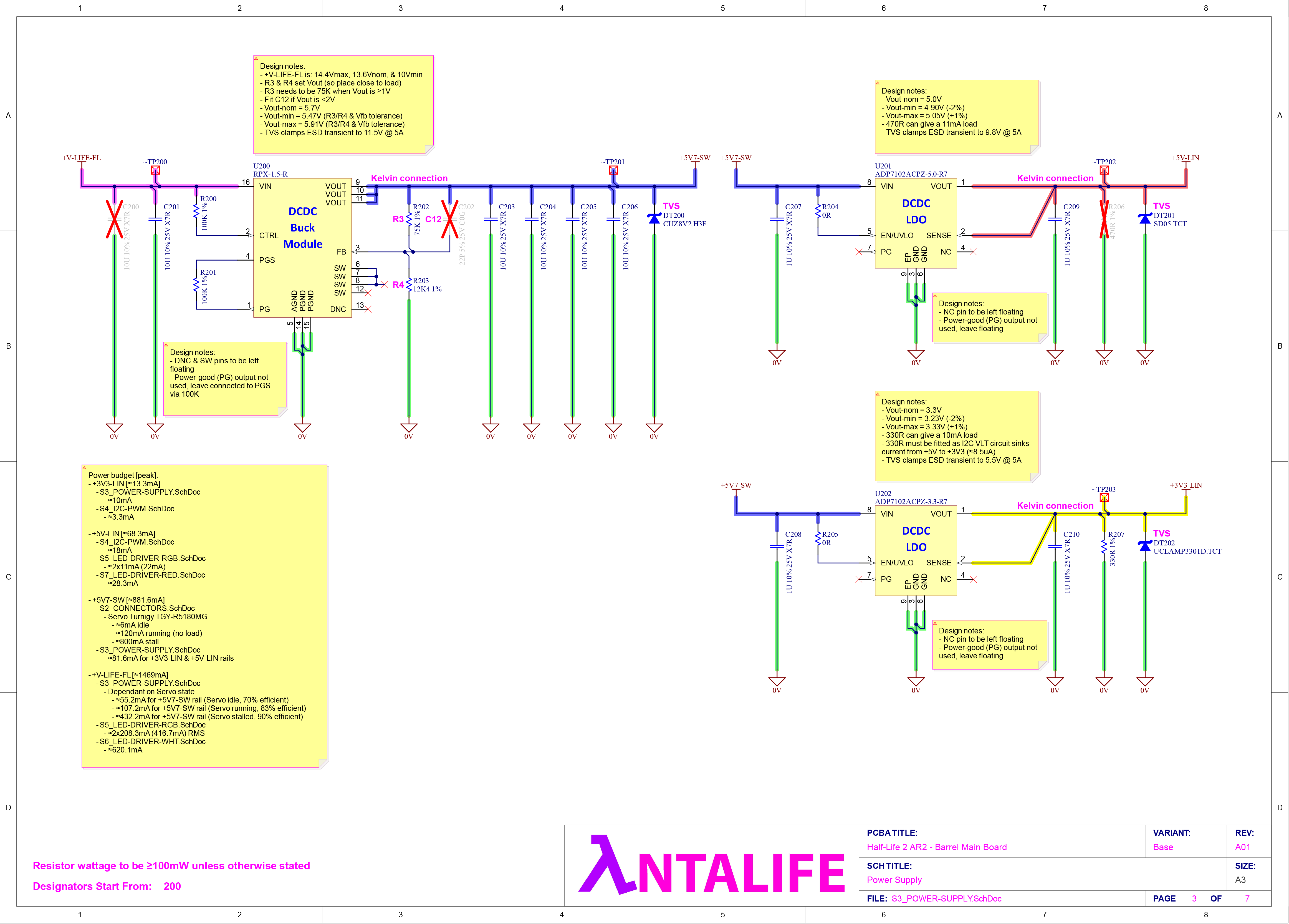
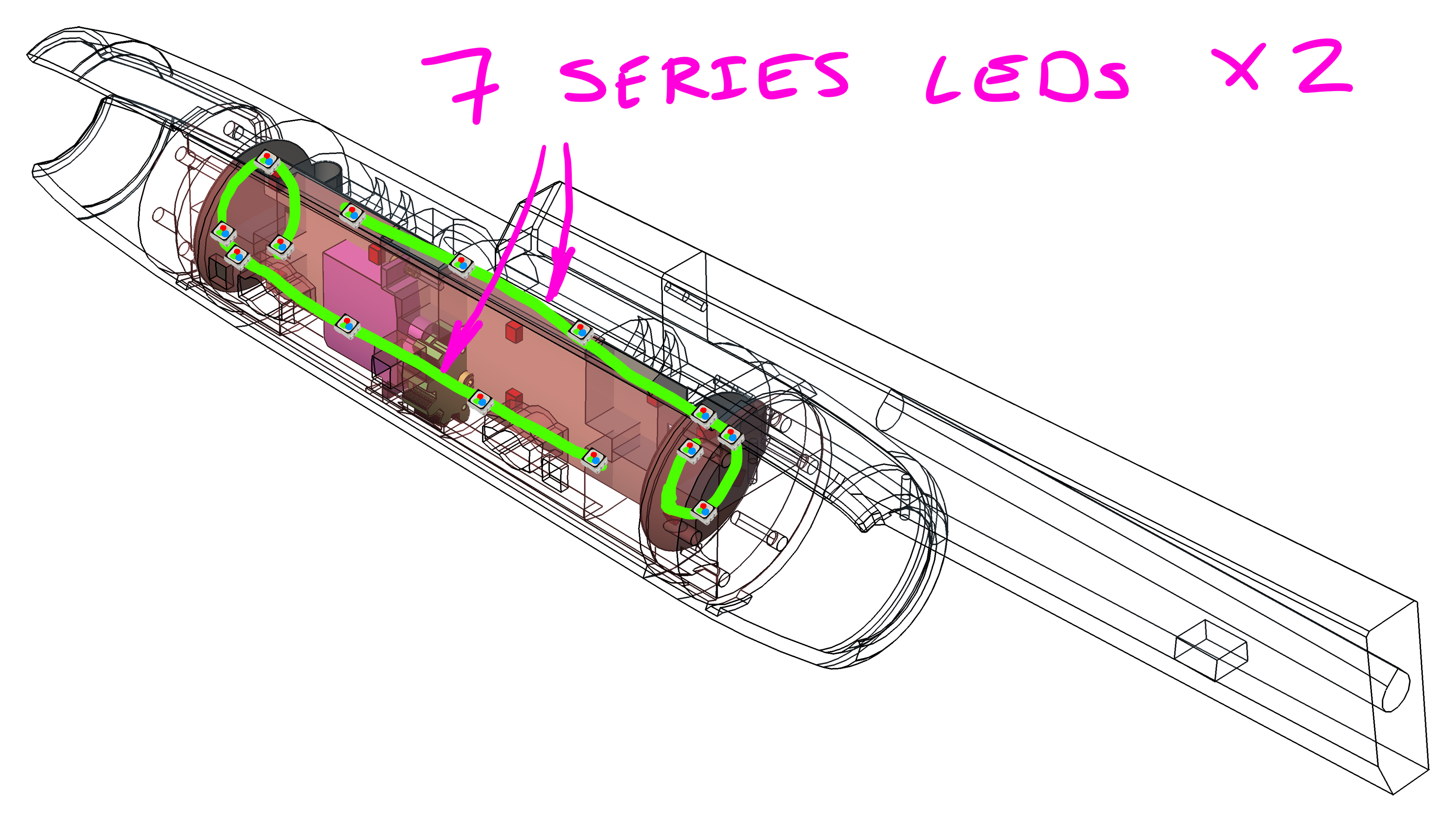
1. AR2 Barrel is nearly complete, just putting on the finishing touches (LED diffusers, shell fingers, spring holder...)


2. Waifu decided to hold her first DnD campaign and asked me to design and 3D print some props


3. Fortifying the work area because someone has learned how to crawl ; - ;

09 October 2022

PROJECT: Half-Life 2 AR2, Update #19 - Barrel Electronics


After many late nights and long train rides the AR2 Barrel electronics are complete! For those curious the electronics assembly consists of 4 PCBAs:


BARREL_MAIN-BOARD

  • The Big Boss
  • Holds various switching & linear regulators that power servo & RED/WHT/RGB LEDs
  • LED brightness/colour & servo position are controlled with PCA9685PW, which itself is controlled via I2C
  • Lastly, as this is the main gateway to other PCBAs (one of which will be over a long cable...), the board has additional filtering & protection to improve EMI & ESD performance


    BARREL_LED-CARRIER-CENTRE

    • Holds a pair of RGB LED chains for barrel glow effect
    • Interfaces to front & rear PCBAs
    • Has some really cool artwork on the silkscreen/overlay ;^)


    BARREL_LED-CARRIER-FRONT

    • Holds RGB & WHT LEDs for barrel glow & muzzle flash effect


    BARREL_LED-CARRIER-REAR

    • Holds RGB & RED LEDs for barrel & shell glow effect


    And here's how the AR2 Barrel MECH & ELEC assembly looks like:


    Deep-dive into BARREL_MAIN-BOARD PCBA

    Just like with the RECEIVER_MAIN-BOARD I want to give a quick rundown of what I am happy with and what I know could be better (you know... have I had more time). But before getting into the nitty gritty here is a cool timelapse of the board being laid out in Altium:


    The Good

    1. GOOD, Solid 0V reference plane for high energy switching zones

    All of my switching regulators and complementary EMI filters are located on the bottom side, away from the "sensitive" digital zones on top layer. ~0.2mm below the bottom layer I have a solid 0V reference plane, ensuring that the high energy current traces have a closely coupled return path (think small current loop area, translating to lower emissions)

    And for those tracks that change their reference plane (as in jump from bottom to top layer), I make sure to use a 1N stitching capacitor to assist with the return path. More on this in the BAD section


    2. GOOD, Better suited bulk capacitors (package wise)

    Previously I was using 0603 sized ceramic capacitors for decoupling, filtering, & general bulk storage. A downside of such a "small" package (depending who you ask) is that with a typical X5R/X7R dielectric the capacitance will be dependant on bias voltage (and temperature), something most manufacturers don't show in their datasheet:

    NOTE: Electrolytic & tantalum capacitors also have this behaviour, and from memory polymer versions of the two are not as impacted. But as always you need to check the datasheet to know what to expect... as you can get drastically different performance with same dielectric material

    Is this a problem? As always, it depends on the application. But here are a couple of solutions/scenarios if I wanted to stick with using a ceramic capacitors:

    1. Use a dielectric that is "independent" on bias voltage or package temperature, like C0G/NP0. This is the way to go when precision is required (say an active filter), BUT be wary that getting a C0G capacitor that is >100N is going to get expensive
    2. Use a physically larger package (1206 instead of 0603) as having more bulk material assists with bias & temperature behaviour, BUT as you can expect this is at the cost of additional board space. Luckily for me I had plenty of that, so I just upped the package size:


    3. GOOD, Better suited EMI filter

    An improvement to my previous design the EMI filter topology has been changed from pi to T. Which is more appropriate when source & load impedances are LOW (like they are here) 


    The Bad

    1. BAD, Top side tracks have a poor reference plane

    I am very happy with my 0V reference plane (bottom side tracks), but I don't have the same enthusiasm for the reference plane used by the top side tracks... as the thing is incredibly choppy:

    What does this mean? Well I can expect to see increased emissions, as the return current for each trace can no longer run directly underneath. James Pawson of Unit 3 Compliance has a really good video on this, but below are some key slides to explain the issue:

    To help this discontinuity in return path I have sprinkled as many reference plane stitching capacitors as I can across the board. But now that I think of it I should have just poured 0V on the top side and stitched it to the internal 0V reference plane with a matrix of vias, spaced to reflect the highest frequency of concern


    2. BAD, LED connector positions could be better

    Though I am quite happy with the tight layout on the bottom side, once the LED related nets make their way to the top side the trace lengths become unpleasantly long due to the connector positions. Again I can expect increased emissions due to the larger loop area D:

    An easy solution would be to move the connectors (not possible), or throw more layers at the board


    3. BAD, EM zone boundary filters could still be better

    J101 could easily have a common mode choke on all 3 data lines, as each pin has a 0V conductor next to them...

    J102, P100, & P101 do not have a filter at all... So expect worse emissions (EM noise getting out) & susceptibility (EM noise getting in) performance here


    Schematic & PCBA

    And to close it all off, here are the BARREL_MAIN-BOARD schematics:


    And the PCBAs

    10 July 2022

    UPDATE: COVID, TV Cabinet, & Half-Life 2 AR2

    COVID

    Life sure has a funny sense of humour, only last week I was having a chat with colleagues about how lucky I have been to have dodge the COVID bullet for so long... and well guess who caught the thing not long after D:

    Recovery wise things are progressing well. I got over the major flu-like symptoms relatively quickly (thanks to the vaccine and booster), and am now left with a blocked nose and a minor loss of smell


    TV Cabinet

    The waifu :3 and I have finalised our biggest (physically and workload wise) wood-working project to date, a TV cabinet. Just like with our Kitchen Shelves the plan is to fasten as many thing as possible with wood joints (vs say wood screws)

    A funny thing that did happened during the SOLIDWORKS assembly check is that we realised there may be a bit of an issue getting the thing in/out of the apartment...

    Lucky for us we realised that we can just stand the bottom cabinet upright and wedge it out of the lounge/entrance-hall bit by bit


    Half-Life 2 AR2

    So what does this all mean for the AR2? Well... we are aiming to finish the TV cabinet this year (and for a really good reason too), meaning work on the AR2 will be slow ; - ;

    BUT that does not mean I am giving up, and right now I am making some slow but steady progress on the AR2 Barrel assembly:

    16 April 2022

    PROJECT: Half-Life 2 AR2, Update #18 - RGB LED Driver Revision


    The last few months have been quite the rollercoaster for us, from Putin's unjust invasion of Ukraine, to me starting a new job... And only recently have I had the headspace to get back to the AR2

    So in this quick update I want to show yous the revised RGB LED driver configuration. Basically I will be halfling the barrel LED zones from 4 (2x3S & 2x4S) to 2 (2x7S). Doing so reduces the complexity of the barrel PCBA's (like halfling the RGB LED driver IC's from 4 to 2, and lowering the LED connector pin-count from 28P to 16P), which is a welcome change as each RGB LED driver (LT3496) goes for ~13AUD/pc in low quantities

    Now you might be asking, why not just drive all the 14 RGB LEDs in a big series configuration? Well I tried to simulate this scenario and soon realised that the forward voltage drop for the big LED chain would be too much for the LT3496 (who's SW pin is rated to 45V). I should also mention that I configure the OVP (Over-Voltage Protection) to 35V, so anytime the SW pin goes beyond this the IC shuts down for that switching cycle. Lastly below is the total forward voltage drop of each LED chain, and as you see in both cases we are over the 45V/35V limit:

    • RED ⇒ 2.6Vf * 14 ⇒ 36.4Vf-tot
    • GRN/BLU ⇒ 3.5Vf * 14 ⇒ 49.0Vf-tot

    While if we break up the chain into half (2x7S) we are nicely under the limit:

    • RED ⇒ 2.6Vf * 7 ⇒ 18.2Vf-tot
    • GRN/BLU ⇒ 3.5Vf * 7 ⇒ 24.5Vf-tot


    So with all that out of the way, here are the latest simulations of the 2x7S RGB LED configuration:


    And here is an updated power losses & expected temperature rise (per IC) table:

    IC Type RθJA, [°C/W] IC losses average, [mW] IC losses maximum, [mW] Temp above ambient, [°C]
    LT3496 Switching 34°C/W RED 68mW
    GRN 57mW
    BLU 57mW
    RED 113mW
    GRN 91mW
    BLU 91mW
    6°C to 10°C


    Couple of interesting things to note with above simulations/table:

    1. I highly suspect that the LTspice model I am using for the BLU/GRN LED is not the best as I am seeing massive ON/OFF & OFF/ON transients (like in orders of 100's of mA). I am certain that the peak current would be more closer to that of the RED LED simulation (~20mA above nominal), but to test this I plan to place an inline 0R jumper which I will then use to measure the actual peaks with a fancy oscilloscope at work
    2. The RED LED channel is showing a higher power loss, this is due to the RED LED current being double that of the GRN/BLU channel (40mA vs 20mA). So think greater I²R losses

    20 February 2022

    PROJECT: Half-Life 2 AR2, Update #17 - RGB LED Driver


    Guess who is back to crunching simulations in LTspice, this time trying to figure out how well the RGB LED driver works ;^)


    RGB LED, Configuration, & Driver Overview

    The RGB LED I have decided to use is the BROADCOM ASMT-YTD7-0AA02, which also comes with a diffused silicone cap to mix the emitted light


    The LEDs will be divided into 4 zones/strings inside the AR2 Barrel:


    Finally, after comparing LED drivers like HV9980, LT3597, LP5009... I decided to settle on the LT3496 to drive the above configuration. The thing that makes this driver special is that it has a Buck-Boost mode, which is a must when the nominal battery voltage hovers close to the total forward voltage of the LED sting (particular for the GRN & BLU channels). Below is the LTspice simulation for the RED string:

    A few key points about this LT3496 configuration:

    1. Reducing the current sense voltage (CTRL pin) from 100mV to 50mV lowers the peak LED current during ON-OFF transition from 110mA to 80mA (think reducing swing range of error amplifier). LEDs are rated for 100mA peak 100ns pulse and though the 110mA pulse was only for 25ns, I really wanted to be sure I am not hitting the 100mA maximum limit
    2. Reducing the switching frequency from 2.1MHz to 1.25MHz improves converter efficiency, as ON losses are lowered from 96mW to 76mW. Reducing the frequency beyond this brings diminishing returns, as losses are more or less ~70mW, while LED ripple current is increased (for same size inductor, 10μH)
    3. Chosen VC filter (22K & 470P) helps minimize LED current overshot and improves settling time (during OFF-ON transition)
    4. OVP resistor divider sets the LED string over-voltage protection to 35V. So if in the unlikely scenario that say a single LED fails in the RED string, the string will be safely shutdown to make sure it does not impact the GRN/BLU strings 


    RGB LED in Detail (Or Why We Need a Buck-Boost Mode)

    Remember when I said having a Buck-Boost mode is super useful when the nominal battery voltage hovers close to the total forward voltage of the LED sting? Well lets look at this in more detail... First off I will be using a 4S LiFePO₄ battery, so I expect the voltage to be:

    • 14.4V maximum
    • 13.6V nominal
    • 10.0V minimum


    I plan to drive each LED channel at 80% maximum DC current rating, so I expect the individual forward voltage to be:

    • RED 2.3Vf nominal @ 40mA, & a maximum of 3.0Vf
    • GRN 3.1Vf nominal @ 40mA, & a maximum of 3.6Vf
    • BLU 3.1Vf nominal @ 40mA, & a maximum of 3.6Vf

    So with a 3 series LED string the forward voltage will be:

    • RED 6.9Vf nominal & 9.0Vf maximum
    • GRN 9.3Vf nominal & 10.8Vf maximum
    • BLU 9.3Vf nominal & 10.8Vf maximum

    And with a 4 series LED string the forward voltage will be:

    • RED 9.2Vf nominal & 12.0Vf maximum
    • GRN 12.4Vf nominal & 14.4Vf maximum
    • BLU 12.4Vf nominal & 14.4Vf maximum

    Note how the LED string forward voltage spans the range of the battery voltage, meaning we can't just use a Buck or Boost regulator, as we will run into cases where battery voltage is too high/low for regulator to function. This is exactly where the Buck-Boost mode saves the day, as it can happily regulate the string voltage to required value :D


    Linear vs Switching (Or When Things Get Hot)

    So first of all we can't use a linear regulator to drive 4 series LEDs, unless we increase the battery voltage (as it would need to be ~2V higher than maximum forward voltage of the string). A linear regulator can just about drive 3 series LEDs, as in this scenario the battery voltage mostly gives enough headroom. With that said, lets compare how a linear regulator compares to a switching one

    NOTE: I am setting the LED string brightness with a 1kHz PWM waveform that is at 50% duty


    So using a switching regulator reduces the average dissipated power by ~70% (from 145mW to 40mW), and the ON dissipated power by ~80% (from 290mW to 56mW)... and that's just for the RED LED string/segment (as in not including the GRN/BLU string)! 

    Next lets expand the simulation to include the GRN/BLU LED driver losses and see what the expected IC (just the one, not the 4 I need to drive all barrel zones) temperature rise above ambient is:

    IC Type RθJA, [°C/W] IC losses average, [mW] IC losses maximum, [mW] Temp above ambient, [°C]
    LP5009 Linear 54°C/W RED 145mW
    GRN 120mW
    BLU 120mW
    RED 290mW
    GRN 239mW
    BLU 239mW
    21°C to 42°C
    LT3496 Switching 34°C/W RED 40mW
    GRN 46mW
    BLU 46mW
    RED 56mW
    GRN 69mW
    BLU 69mW
    5°C to 7°C


    And with all that waffle out of the way... we can see that using a switching regulator is the way to go, as:

    1. It is more energy efficient, resulting in a cooler AR2 Barrel ;^)
    2. It can actually drive 4 or more RGB LEDs in series, while being powered from same 4S LiFePO₄ battery