Many things have happened since the last update, the biggest of which being that the Neato D5 Mod PCBA (aka Neato Lupin Mod) is now obsolete as the Vacuula (formerly Brainslug) team have figured out how to run custom FW on the existing Neato Botvac HW :D
I had lots of fun with this project, so I'm making this last post to close things off.
The FW required the modification below to improve WiFi stability on the XIAO ESP32-C6 module. I highly suspect this is related to the +3.3V rail drooping (brownout) during WiFi Tx, as I am powering the module directly from the debug port +3.3V output. Not ideal... but it's the best I could do without breaking into a +5V rail on the Neato Botvac mobo.
I did try monitoring the +3.3V rail with rev B01 PCBA (with the help of a precision +1.024V reference for ADC read calibration), but as expected the ADC sampling was too slow to capture any meaningful data. Ideally I should have been using an oscilloscope with a current probe.
Neato Media:
Rev A01 PCBA shape & bend simulation in Altium Designer. The purple region is rigid FR4 stiffener.
I though I had it all figured out and ordered the above FPC (Flexible Printed Circuit) from JLCPCB. Then I assembled it and found that the bottom half collided with the Neato D5 bumper... guess who forgot to do a visual (printed paper) & virtual (SolidWorks) check with the bumper installed D:
So this time I made sure to check things properly before ordering the rev B01 FPC:
Once the FPCs arrived, I then assembled them using the Miniware MHP30. Below is a sped-up video (x10) of the solder reflow process. Left is digital microscope,
right is thermal cam. Interesting how the hotplate temperature increases like wave:
And finally, here is the modded Neato Botvac D5. Ready to keep our place clean for that bit longer:
After joining the Neato Connected Discord I ran into another smart banana (4_Fools) that proposed hiding the ESP32 behind the bumper and running a ribbon cable to the debug port like so:
So I plonked a Seeed ESP32-C6 (since they are known for quality HW, especially when speccing the internal antenna) and a generic 4P 0.1" female socket into the SolidWorks assembly and yea this looks like the best way to go, as it's a plug & play mod that (hopefully) does not require any modifications to the bumper:
Next step is to figure out the flex shape and reach out to JLCPCB for their flex, rigid stiffener, & adhesive spec.
First and last post of 2025... We on toddler time now fam :D
ISSUE:
Now that Neato has finally kicked the bucket (and all robot vacuums of their
servers), our much loved D5 has become a bit less useful. We can still push the power button to start a manual (and unoptimized) route, but can't do so remotely... So no more vacuuming the house twice when we are out and about D:
IMMEDIATE FIX:
Continue using manual route until... (see below).
PROPOSAL:
Luckily some very smart bananas (Philip2809) have figured out that you can control the D5 (and many other models) via the debug port with the help of an ESP32 & Home Assistant. Currently interfacing to the debug port is done in two ways, the first looking quite cyberpunk and the latter requiring you to disassemble the whole robot:
But I though, why not have a bit more fun with it and design my own rigid-flex PCBA that sits nicely on the bumper. Initially I was thinking of placing
the PCBA and cover on the top of bumper and running the flex underneath, but I
soon found that there is a pinch point where the flex would exit. Plus
there would be some tight bend radiuses which are far from ideal for a continuously (though minor) moving assembly:
Then I though about placing it on the side (position 2 below), but this would
mean the right side of robot would not be able to run as close to the wall as
before. So the next best position is at the front of
the bumper, directly above the debug port (position 3 below). Sure this loses
a bit of front bumper space, but it does mean the flex region of PCBA is short
and does not have any complex bends:
DECISION:
Front of bumper (position 3) it is. Next step, figure out rigid-flex PCBA
constrains from my very crude 3D scan (which you can get here):
After many late nights and long train rides the
AR2 Barrel
electronics are complete! For those curious the electronics assembly consists
of 4 PCBAs:
BARREL_MAIN-BOARD
The Big Boss
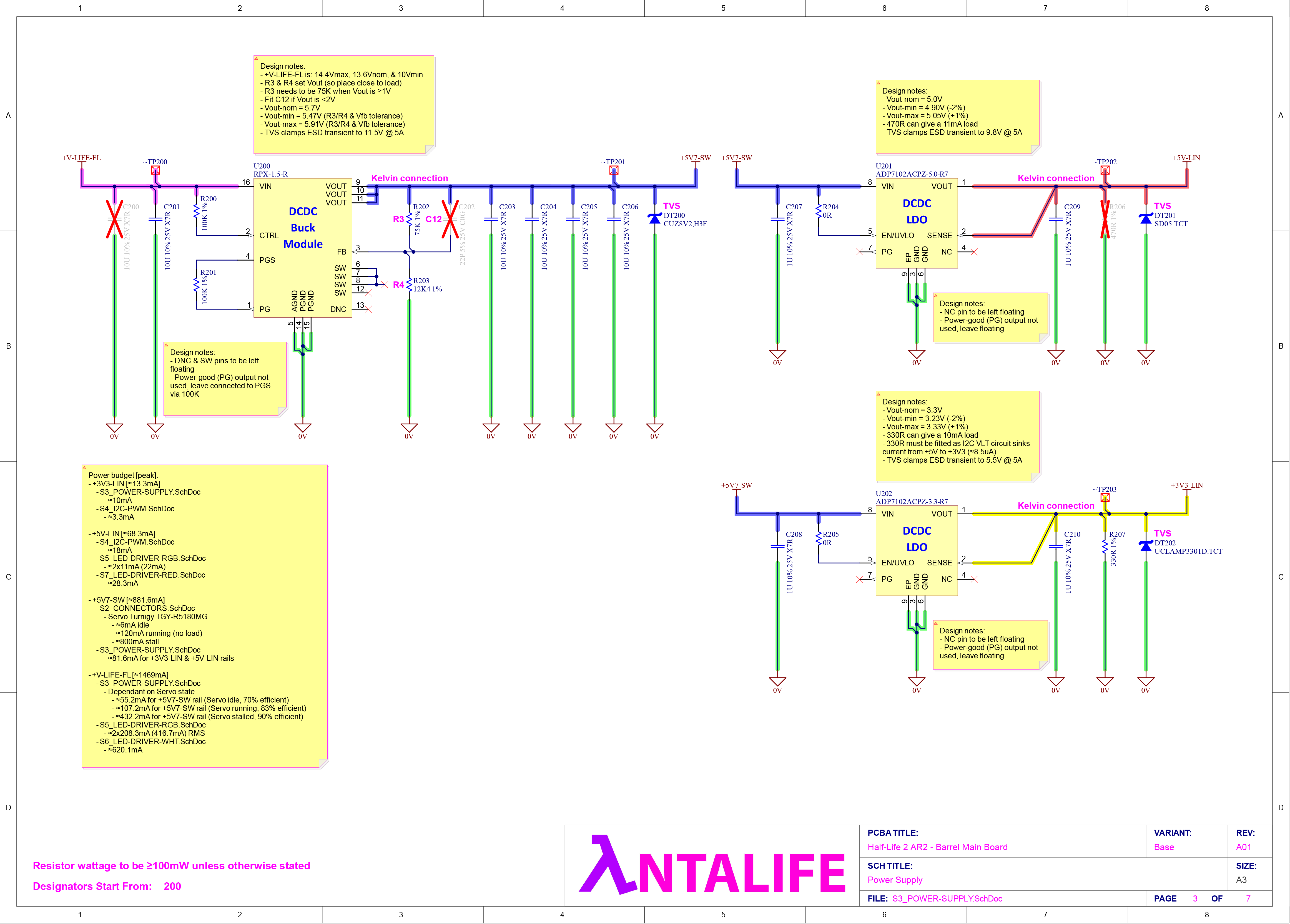
Holds various switching & linear regulators that power servo &
RED/WHT/RGB LEDs
LED brightness/colour & servo position are controlled with PCA9685PW, which itself is controlled via I2C
Lastly, as this is the main gateway to other PCBAs (one of which will be
over a long cable...), the board has additional filtering & protection
to improve EMI & ESD performance
BARREL_LED-CARRIER-CENTRE
Holds a pair of RGB LED chains for barrel glow effect
Interfaces to front & rear PCBAs
Has some really cool artwork on the silkscreen/overlay ;^)
Holds RGB & RED LEDs for barrel & shell glow effect
And here's how the AR2 Barrel MECH & ELEC assembly looks like:
Deep-dive into BARREL_MAIN-BOARD PCBA
Just like with the RECEIVER_MAIN-BOARD
I want to give a quick rundown of what I am happy with and what I know
could be better (you know... have I had more time). But before getting
into the nitty gritty here is a cool timelapse of the board
being laid out in Altium:
The Good
1. GOOD, Solid 0V reference plane for high energy switching zones
All of my switching regulators and complementary EMI filters are located
on the bottom side, away from the "sensitive" digital zones on top layer.
~0.2mm below the bottom layer I have a solid 0V reference plane, ensuring
that the high energy current traces have a closely coupled return path
(think small current loop area, translating to lower emissions)
And for those tracks that change their reference plane (as in jump from
bottom to top layer), I make sure to use a 1N stitching capacitor to
assist with the return path. More on this in the BAD section
Previously
I was using 0603 sized ceramic capacitors for decoupling, filtering, &
general bulk storage. A downside of such a "small" package (depending who
you ask) is that with a typical X5R/X7R dielectric the
capacitance will be dependant on bias voltage (and temperature), something most manufacturers don't show in their
datasheet:
NOTE: Electrolytic & tantalum capacitors also have this
behaviour, and from memory polymer versions of the two are not as impacted.
But as always you need to check the datasheet to know what to expect... as
you can get drastically different performance with same dielectric material
Is this a problem? As always, it depends on the application. But here are a
couple of solutions/scenarios if I wanted to stick with using a ceramic
capacitors:
Use a dielectric that is "independent" on bias voltage or package
temperature, like C0G/NP0. This is the way to go when precision is
required (say an active filter), BUT be wary that getting a C0G capacitor
that is >100N is going to get expensive
Use a physically larger package (1206 instead of 0603) as having more bulk
material assists with bias & temperature behaviour, BUT as you can
expect this is at the cost of additional board space. Luckily for me I had
plenty of that, so I just upped the package size:
1. BAD, Top side tracks have a poor reference plane
I am very happy with my 0V reference plane (bottom side tracks), but I
don't have the same enthusiasm for the reference plane used by the top
side tracks... as the thing is incredibly choppy:
What does this mean? Well I can expect to see increased emissions, as the
return current for each trace can no longer run directly underneath. James Pawson of Unit 3 Compliance has a really good video on this, but below are some key slides to
explain the issue:
To help this discontinuity in return path I have sprinkled as many reference
plane stitching capacitors as I can across the board. But now that I think
of it I should have just poured 0V on the top side and stitched it to the
internal 0V reference plane with a matrix of vias, spaced to reflect the
highest frequency of concern
2. BAD, LED connector positions could be better
Though I am quite happy with the tight layout on the bottom side, once the
LED related nets make their way to the top side the trace lengths become
unpleasantly long due to the connector positions. Again I can expect
increased emissions due to the larger loop area D:
An easy solution would be to move the connectors (not possible), or throw
more layers at the board
3. BAD, EM zone boundary filters could still be better
J101 could easily have a common mode choke on all 3 data lines, as each pin
has a 0V conductor next to them...
J102, P100, & P101 do not have a filter at all... So expect worse
emissions (EM noise getting out) & susceptibility (EM noise getting in)
performance here
Schematic & PCBA
And to close it all off, here are the BARREL_MAIN-BOARD schematics: