LINK TO PREVIOUS POST
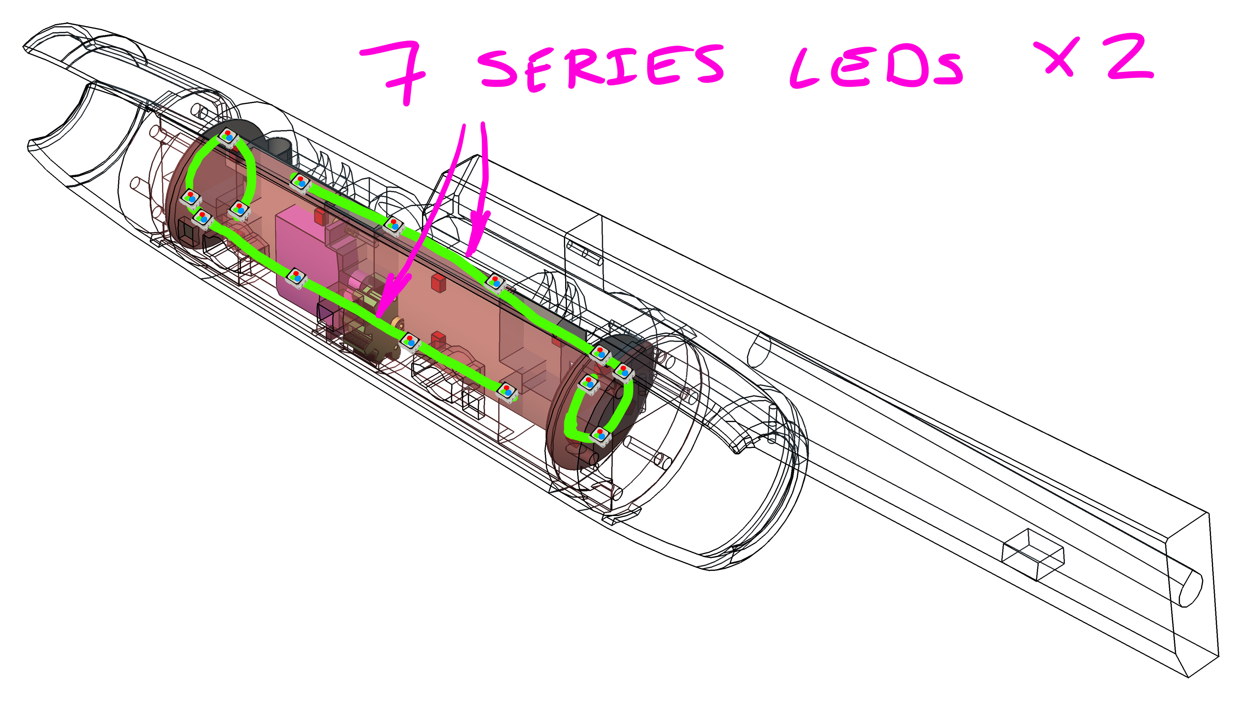
I have completed designing the RECEIVER_MAIN-BOARD, a board that controls all AR2 reciever function. Below is a reminder of
where the board lives, how it looks (banana for scale included), as well as
what the
3 receiver boards
replace on the
AR2 prototype:


Key specs for RECEIVER_MAIN-BOARD:
- 4 layers (signal, 0V, PWR, & signal)
-
All function (including external daughter boards) controlled by a single I²C
line
- Houses a bunch of goodies like:
-
Switching to convert 13.2V to 4.3V (MAXM15462)
-
Linear to convert 4.3V to 3.3V (ADP7102)
-
Low RDSON MOSFET (BSC040N10NS5) based solenoid driver, with the MOSFET being driven by UCC27533
to further reduce power losses
-
ADS7138 to read the analog/digital inputs and/or set digital outputs
Next up I will go over the good & bad design elements... Spoiler alert,
most of it is OK, some of it is meh D:
The Good
1. GOOD, Input filters on all connectors
All nets coming in/out of board (as in nets transitioning the EM zone
boundary, as Keith Armstrong would put it) go through a filter. For example:
-
All logic nets pass through IP4252CZ8-4-TTL,13, a neat ESD filter that uses the diode junctions to form a low-pass RC
filter

Deploying these sorts of filters is a good way of protecting your device
from ESD as well as improving your chances of passing EMC (think slowing
down those fast edges)... BUT the topology I used has room for improvement
as I will discuss in the bad parts section
2. GOOD, Reduced loom conductors
RECEIVER_MAIN-BOARD houses 5 key signals which control all reciever
function. Meaning if I was to control the reciever directly then my cable
loom would need to have 5 IO conductors, not including the return path for
each...
I already have bugger all room in the AR2 so this would be a pain. Instead I
feed the key nets into the ADS7138, an I²C IO expander with ADC functionality. Doing so reduces the loom "IO"
conductor count to 2, which is basically the I²C data & clock line
(again not including the return for each)
BONUS:
-
ADS7138 function could be implemented using a MCU, but that would mean I
would have one additional thing to program and test... So to reduce
complexity it's way easier to use an off the shelf IC that contains
everything I want
3. GOOD, Efficient 13.2V to 3.3V conversion
Majority of reciever boards are powered by 3.3V, with the only exception
being the solenoid which is powered "directly" from the LiFePO₄ battery (as
in 13.2V). Also here is the power budget for all reciever boards:

The question then becomes how to covert 13.2V to 3.3V? Here are 3 common
ways of solving this:
- Use a linear (or LDO) regulator
- PRO: Super quiet 3.3V rail
- CON: Efficiency will be 25%, so will have to dissipate 0.38W
- Use a switching (or SMPS) regulator
-
PRO: Efficiency will be 85%, translating to a power loss of 0.02W (as in
bugger all)
-
CON: 3.3V rail is not quiet, expect 10-50mV ripple depending on load
- Use both ;^)
-
PRO: Overall efficiency will be ~77% (0.07W loss), and ripple will be
non-existent
- CON: Additional complexity, cost, and board real-estate
I would have probably been OK with option 2, but I wanted to try something
new so went with option 3:

But why use 4.3V as the intermediate rail? Well there were two factors
I tried balancing:
-
To have a high LDO efficiency (at a given current) your input voltage
should be as close as possible to the output voltage (think lower "voltage
drop")
-
To have a high PSRR (at a given current) your input voltage should be as far as
possible from the output voltage (think having a greater buffer to reject
all that ripple)
From the gif below you can see that PSRR for 4.8V & 4.3V is identical,
while for 3.8V it get's a tiny bit worse. Hence why I went with 4.3V

BONUS:
- Am using a couple of TVS diodes to protect the key rails
4. GOOD, Reference plane stitching CAP's
Because I am using a cheap 4L stack-up I am limited to two different
potential reference planes:
- 0V, used as top copper reference
- 3.3V, used as bottom copper reference
A few of my tracks jump from top to bottom and in the process change their
reference plane. To help make their return path continuous (think reducing
radiated emissions due to odd return paths) I have stitched the two
reference planes where the layer change occurs with 1N 5% 25V C0G
capacitors:

One thing to note is that had I used a thinner 4L stack-up (as in one where
0V & 3.3V planes are ~0.2mm from one another), then I would not have
needed the stitching capacitors

5. GOOD, Adequate cooling for MOSFET
Having such a tiny board does not leave much space for cooling the MOSFET
(BSC040N10NS5), which according to the datasheet has a thermal resistance of 50K/W for a
6cm² area. The most I can give it is ~3cm², and that's split up over top
& bottom copper:

So I am expecting the thermal resistance to be ~100K/W, which seems to be
enough as at full load (10A continuous) the MOSFET is expected to operate at
~35°C above ambient. Actual rise will likely be slightly lower as I am
pulsing the MOSFET at ~7Hz
BONUS:
-
The top & bottom "heatsink planes" are stitched together with x12
0.4mm diameter vias
-
I could add more but I would be getting to the point of diminishing
returns

The Bad
1. BAD, Input filters on all connectors could be better
To improve radiated immunity (especially for a multi-board design) I
need to pass all nets coming in/out of board through a common mode choke
as soon as they transit into EMZ1. This would stop any transient
voltages (say from a near ESD event) creating transient currents in the
conductors, and confusing what each board considers 0V to be:

Next up, the 10A pi-filter I am using is not ideal as both source and load impedances are
LOW, where as a pi-filter is better when both are HIGH:

2. BAD, Tack & pad clearance to reference plane edge
Current board envelope is the largest I have space for in the reciever,
and even with that I am forced to cram component pads and tracks right
up to the reference plane edge. If I had more space I should space the
tracks & pads to be at least 3mm away from reference plane edge,
otherwise I can expect to have worse EMC performance...

3. BAD, Board is not designed for manufacture ;^)
This one is not a huge issue as I will be assembling the board myself.
But if I was to revise the board to make it more suitable for
manufacture, I would:
-
Add fiducials, so that pick and place machine has an accurate
reference point
-
Move SMD components to be at least 2-3mm away from board edge, so that
pick and place machine can actually clamp the board. Otherwise give
the board a meaty panel

Schematic
And for those curious here are the schematics so far: